Inorganic molecules that form helical shapes have potential to break transistor size limits
As computers have progressed over the last few decades, with their component transistors getting ever smaller and ever more numerous on a single chip, that relentless progress, famously described by Moore’s Law, has begun to bump up against fundamental physical limits to what can be done with the present etched-lines-on-silicon technology. But now, a new twist involving an inorganic molecule that has a DNA-like helical shape may provide an alternative pathway that could shrink transistors down to atom-sized scales. And even DNA molecules themselves might ultimately become the bits and bytes and logic gates of the future.
Transistors are the fundamental building blocks of computer chips, just as proteins are the basis of living organisms. They are essentially just sophisticated on–off switches, whose state can be flipped from one to the other by applying an electrical signal, or boosters that can amplify a signal. Arranged together in complex circuits, they can store the ones and zeroes of computational data, or carry out the basic logic functions (AND, OR, etc.) that underlie all computation. The first computer chips had dozens of transistors on them, but nowadays they each contain billions.
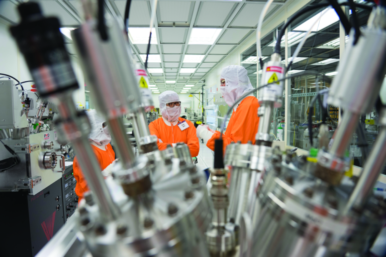
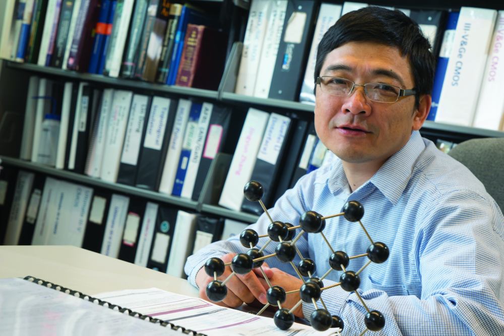
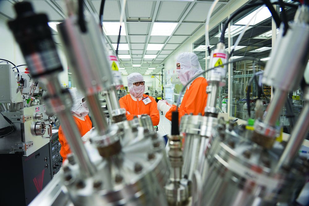
But the constant shaving down of the sizes of transistors and the wires that interconnect them on a chip have now made them so tiny that random quantum effects are beginning to limit any further shrinkage. Whole new pathways are needed, and researchers around the world are pursuing a wide variety of approaches to overcome these limits. One of the more unusual projects is taking shape at Purdue University, where Prof. Peide Ye (Figure 1), in collaboration with researchers at other universities, is exploring the potential of a metallic element called tellurium.
Using rare-earth metals
Tellurium, the team found, has a highly unusual property. Unlike so-called two-dimensional materials such as graphene and boron nitride, which naturally form into sheets just a single atom or two thick that have unique properties, under special conditions tellurium can form into what are essentially one-dimensional forms: Single atoms in a kind of daisy chain, each holding onto one other neighboring atom, and forming a stack of slightly offset pairs.
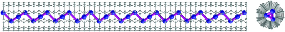
And that’s where the twist comes in: these single-chain arrays of tellurium atoms don’t form a straight line. Rather, it forms a stack of pairs that just naturally twists into a helical form, reminiscent of DNA molecules or the steps of a spiral staircase. But unlike DNA, which only goes one way, tellurium has no preference for whether the helix turns clockwise or counterclockwise, so the two forms are produced in equal measure.
Tellurium, being metallic, is naturally conductive. When encased in a nanotube of a nonconductive material, for which Ye and his team used boron nitride, the pair of materials form a junction that can act as a field effect transistor, the team found.
Ye, who is the Richard E. and Mary Jo Schwartz Professor of Electrical and Computer Engineering at Purdue, says these tellurium helixes in their boron nitride nanotubes have the potential to be the smallest transistors ever made (Figure 2). The entire transistor structure can be just two nanometers across, while today’s smallest silicon transistors range from 10 to 20 nm.
Many teams around the world are working on a wide variety of ultrathin materials, Ye says, in hopes of finding replacements for the silicon in the microchips that increasingly are at the heart of nearly everything we use, from smart phones and laptop computers to biomedical diagnostic and treatment devices to smart thermostats, appliances, and light bulbs. But Ye and his coresearchers, including some at Michigan Technological University, Washington University in St. Louis, and the University of Texas in Dallas, say tellurium is one of the most promising. They published their initial results in the journal Nature Electronics earlier this year, demonstrating working transistors built on this principle.
Ye didn’t originally set out to create a helical material, or even a one-dimensional one.
The initial research was aimed at creating new 2-D materials, to build upon the existing arsenal of materials such as graphene, which is pure carbon in a hexagonal lattice, or silicine, stanine or borophene, or hexagonal boron nitride, or a family of materials known as transition metal chalcogenides. They worked to create a 2-D form of pure tellurium, and succeeded in 2018, producing a new material called tellurene.
But the team pushed further, probing to see what other interesting properties tellurium might yield for electronics. Three Purdue doctoral students led the search for a one-dimensional form of the element, which is part of the rare-earth group, and for a way to make transistors from it.
“We realized tellurium is fundamentally not a two-dimensional material, but a one-dimensional material,” Ye says. But when the team succeeded in building single-atom-wide chains, by growing them inside carbon nanotubes, they were surprised to discover that the chains wound themselves up in the helical “snake like” form instead of forming straight lines, as expected, he says (Figure 3).
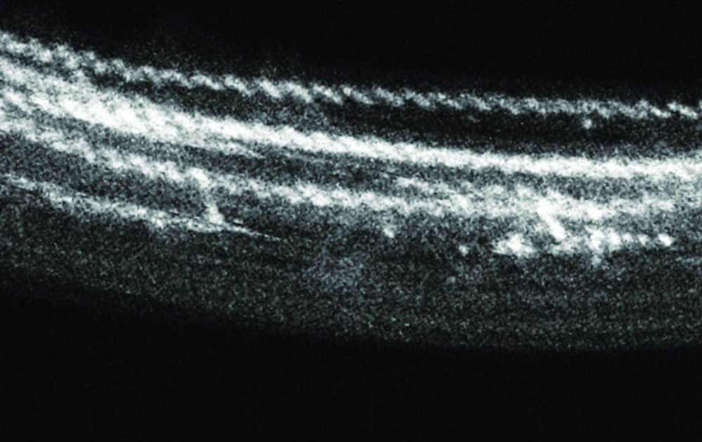
Researchers at Purdue and the University of Texas at Dallas were able to image the materials using transmission electron microscopy (TEM), proving the chain-like material’s helical structure, which is based on stacks of two-atom pairs whose layers are bound together by Van der Waals forces (Figure 4). These pairs then arrange themselves into a helix just as the base pairs in a DNA helix do. “It was very challenging to take a picture of this chain of atoms,” Ye says. But the structure “is an inherent property of these atoms.”
Carbon nanotubes are conductive, however, so the original configuration of tellurium chains inside carbon nanotubes would not allow for a functioning transistor, which would need to be electrically isolated from its environment. To form functioning transistors, the 1-D tellurium chains would need to be grown inside nonconductive casings instead. Fortunately, there is such a thing.
For that, the team turned to Yoke Khin Yap at Michigan Technological University, who provided a variety of nanotubes made of boron nitride, a naturally insulating compound that readily forms 2-D sheets and nanotubes. These nanotubes took the place of the carbon-based ones and the tellurium chains were grown inside them.
While trapping a single tellurium 1-D strand would require a nanotube just 0.8 nm across, the boron nitride nanotubes they used only go down to about 2 nm across, so the testing involved tubes containing several strands rather than just one.
While bigger than the ideal single-strand helix transistor, the multistrand version is still small enough to handily beat other transistor technologies in the race to the bottom in scaling down microchips, Ye says. “Even if you have a few of these strands, you still have the smallest transistor,” he says. But he continues to work on ways of further improving the system.
The research so far has not produced any ways of specifically making use of the difference between the two mirror-image versions of the helical structure. But if some chemical or electrical system could separate the two forms to make use of the difference, perhaps it could provide a way of encoding additional information in each strand. “We’re working on that,” Ye tells IEEE Pulse.
Another direction the team is pursuing is the use of selenium atoms instead of tellurium, which may turn out to have similar properties. But it is more difficult to handle, Ye says.
Already, some companies are working to develop the technology further, Ye says. The U.S. Defense Department, which partly funded the research, is interested in research on a variety of silicon alternatives. But the concept is still a lab-scale project, with a great deal of development needed before it could become a practical product, though there may be some niche applications that could be implemented sooner.
DNA origami
Meanwhile, other teams around the world continue to explore yet another alternative to silicon for smaller and faster computers—the possibility of using DNA molecules themselves for computation. This would take advantage of some of the built-in capacity for replication and self-repair that these biomolecules offer. Such efforts have been going on since at least the 1990s, with much interesting research but so far no clear application that provides advantages over other materials.
Researchers at Israel’s Weizman Institute produced some of the earliest DNA- and enzyme-based computers, and in 2004 Ehud Shapiro and a team of others at Weizman made a DNA computer capable of assisting with cancer diagnoses. By 2013, researchers succeeded in storing large amounts of data in the form of DNA storage. Research continues toward truly reversible, flexible computational tools making use of DNA, but that goal has remained elusive. Lab-scale devices have been developed, but nothing has yet reached commercial application.
The quest continues, though, because theoretical calculations have shown that in principle, an amount of DNA-based material smaller than a typical PC could be many orders of magnitude faster and store orders of magnitude more data than all the computers ever built, some researchers have estimated.
John Reif, a distinguished professor of computer science at Duke University, is one of the leaders in this area of research. His recent work has focused on fast and compact DNA logic circuits, DNA-based digital data storage, DNA barcodes for single-molecule fingerprinting, and DNA-based analog computing.
Some of this research is focused on using the ability of DNA molecules to bind to one another to create complex shapes. These can aid in the diffusion process of DNA strands—which is one of the limiting factors in DNA computing. Though the diffusion is very slow by computing standards, it is counterbalanced by the extraordinary parallelism made possible by its tiny, easily replicable molecules. A whole field of DNA origami has arisen, using shapes constructed from DNA chains as a way of speeding the diffusion process, and many other functions.
In principle, DNA computing could have many advantages. The material itself is abundant and cheap, and unlike many of the materials now used in microchip manufacturing, there’s nothing toxic or hazardous about it or the materials used to handle it. And in principle it can beat just about anything in terms of computational power for a given weight or volume.
Last year, for the first time, a DNA computer was demonstrated by Prof. David Doty at the University of California at Santa Cruz that could actually be reprogrammed. Until then, every DNA computer was hardwired with its instructions and could only run a single algorithm, Doty said, but the new device opens the door to potential multipurpose DNA computing.
Doty suggested the programmable DNA devices could be used to program DNA robots, which in turn could be used for example to target specific cancers in the body. The research, described last year in Nature, is still very basic and exploratory, and far from any practical application. But it is perhaps the most promising sign so far that the untapped potential of DNA computing might be on the horizon.
Whether it’s in the form of some kind of reprogrammable DNA-based computers, or in the form of transistors made from elemental materials whose natural structures mimic those of the DNA molecule, it seems likely that some kind of helical molecules will be playing an important part in the future of computation and electronics.
For more information
J.-K. Qin et al., “Raman response and transport properties of tellurium atomic chains encapsulated in nanotubes,” Nature Electron., vol. 3, pp. 141–147, Feb. 2020. [Online]. Available: https://www.nature.com/articles/s41928-020-0365-4
J. Reif et al., “Autonomous programmable biomolecular devices using self-assembled DNA nanostructures,” in Proc. Int. Workshop Logic, Language, Inf., Comput., 2007, pp. 297–306, doi: 10.1007/978-3-540-73445-1_21.
D. Woods et al., “Diverse and robust molecular algorithms using reprogrammable DNA self-assembly,” Nature, vol. 567, pp. 366–372, Mar. 2019. [Online]. Available: https://idp.nature.com/authorize/casa?redirect_uri=https://www.nature.com/articles/s41586-019-1014-9